- 您现在的位置:买卖IC网 > Sheet目录480 > MTD6N15T4 (ON Semiconductor)MOSFET N-CH 150V 6A DPAK
�� �
�
�MTD6N15�
�Power� Field� Effect� Transistor�
�DPAK� for� Surface� Mount�
�N� ?� Channel� Enhancement� ?� Mode� Silicon� Gate�
�This� Power� FET� is� designed� for� high� speed,� low� loss� power�
�switching� applications� such� as� switching� regulators,� converters,�
�solenoid� and� relay� drivers.�
�http://onsemi.com�
�Features�
�?� Silicon� Gate� for� Fast� Switching� Speeds�
�?� Low� R� DS(on)� —� 0.3� W� Max�
�?� Rugged� —� SOA� is� Power� Dissipation� Limited�
�?� Source� ?� to� ?� Drain� Diode� Characterized� for� Use� With� Inductive� Loads�
�?� Low� Drive� Requirement� —� V� GS(th)� =� 4.0� V� Max�
�?� Surface� Mount� Package� on� 16� mm� Tape�
�?� Pb� ?� Free� Package� is� Available�
�V� (BR)DSS�
�150� V�
�G�
�R� DS(on)� MAX�
�0.3� W�
�N� ?� CHANNEL�
�D�
�I� D� MAX�
�6.0� A�
�MAXIMUM� RATINGS�
�S�
�Rating�
�Symbol�
�Value�
�Unit�
�4�
�Drain� ?� Source� Voltage�
�Drain� ?� Gate� Voltage� (R� GS� =� 1.0� M� W� )�
�V� DSS�
�V� DGR�
�150�
�150�
�Vdc�
�Vdc�
�1� 2�
�3�
�Gate� ?� Source� Voltage�
�?� Continuous�
�?� Non� ?� Repetitive� (t� p� ≤� 50� m� s)�
�Drain� Current� ?� Continuous�
�Drain� Current� ?� Pulsed�
�Total� Power� Dissipation� @� T� C� =� 25� °� C�
�Derate� above� 25� °� C�
�Total� Power� Dissipation� @� T� A� =� 25� °� C�
�Derate� above� 25� °� C� (Note� 1)�
�Total� Power� Dissipation� @� T� A� =� 25� °� C�
�(Note� 1)�
�Derate� above� 25� °� C� (Note� 2)�
�V� GS�
�V� GSM�
�I� D�
�I� DM�
�P� D�
�P� D�
�P� D�
�±� 20�
�±� 40�
�6.0�
�20�
�20�
�0.16�
�1.25�
�0.01�
�1.75�
�0.014�
�Vdc�
�Vpk�
�Adc�
�W�
�W/� °� C�
�W�
�W/� °� C�
�W�
�W/� °� C�
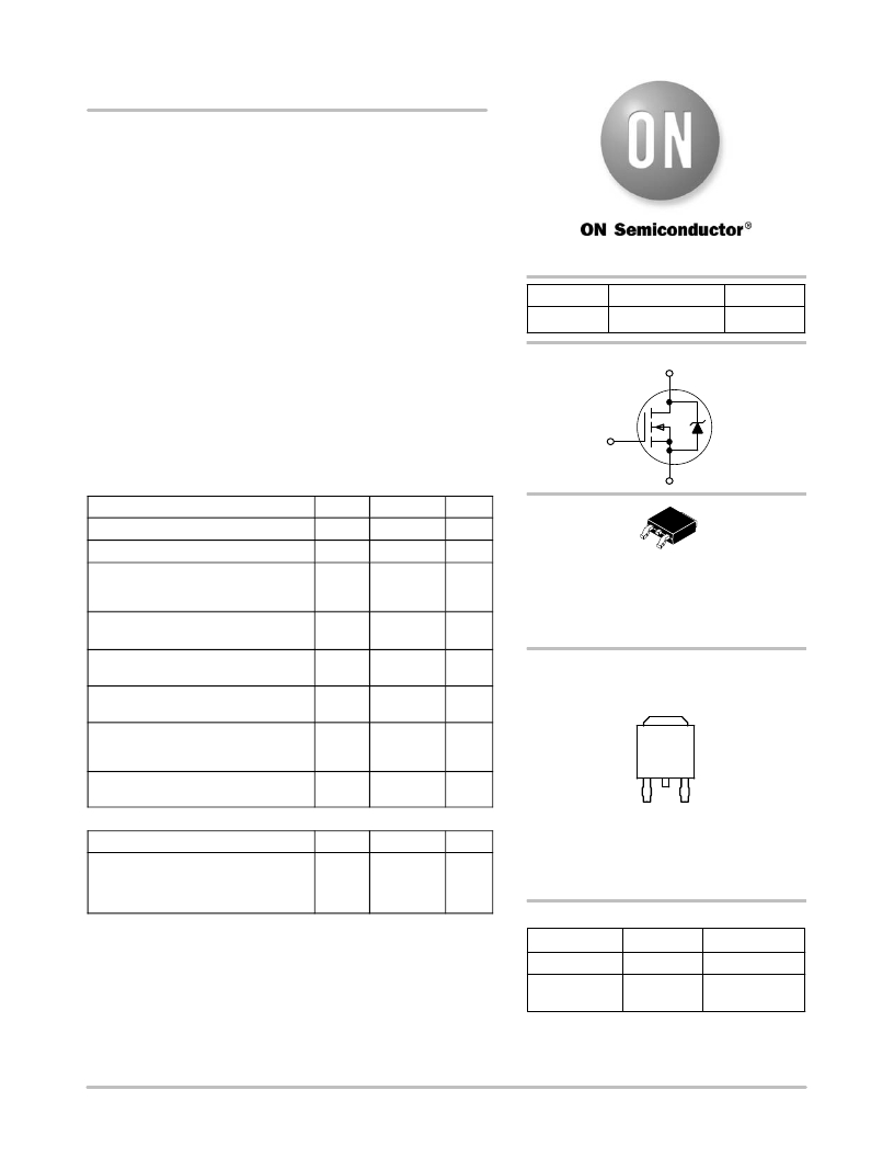
�CASE� 369C�
�DPAK�
�(Surface� Mount)�
�STYLE� 2�
�MARKING� DIAGRAM�
�&� PIN� ASSIGNMENTS�
�4� Drain�
�Operating� and� Storage� Junction�
�Temperature� Range�
�THERMAL� CHARACTERISTICS�
�T� J� ,� T� stg�
�?� 65� to� +150�
�°� C�
�1�
�Gate�
�2�
�Drain�
�3�
�Source�
�Characteristic� Symbol� Value� Unit�
�Thermal� Resistance� °� C/W�
�?� Junction� ?� to� ?� Case� R� q� JC� 6.25�
�?� Junction� ?� to� ?� Ambient� (Note� 1)� R� q� JA� 100�
�?� Junction� ?� to� ?� Ambient� (Note� 2)� R� q� JA� 71.4�
�Stresses� exceeding� Maximum� Ratings� may� damage� the� device.� Maximum�
�Ratings� are� stress� ratings� only.� Functional� operation� above� the� Recommended�
�Operating� Conditions� is� not� implied.� Extended� exposure� to� stresses� above� the�
�Recommended� Operating� Conditions� may� affect� device� reliability.�
�1.� When� surface� mounted� to� an� FR4� board� using� the� minimum� recommended�
�pad� size.�
�2.� When� surface� mounted� to� an� FR4� board� using� 0.5� sq.� in.� drain� pad� size.�
�Y� =� Year�
�WW� =� Work� Week�
�6N15� =� Device� Code�
�G� =� Pb� ?� Free� Package�
�ORDERING� INFORMATION�
�Device� Package� Shipping� ?�
�MTD6N15T4 DPAK 2500/Tape & Reel�
�MTD6N15T4G� DPAK� 2500/Tape� &� Reel�
�(Pb� ?� Free)�
�?For� information� on� tape� and� reel� specifications,�
�including� part� orientation� and� tape� sizes,� please�
�refer� to� our� Tape� and� Reel� Packaging� Specification�
�Brochure,� BRD8011/D.�
�?� Semiconductor� Components� Industries,� LLC,� 2013�
�May,� 2013� ?� Rev.� 5�
�1�
�Publication� Order� Number:�
�MTD6N15/D�
�发布紧急采购,3分钟左右您将得到回复。
相关PDF资料
MTD6N20ET4
MOSFET N-CH 200V 6A DPAK
MTD6P10E
MOSFET P-CH 100V 6A DPAK
MTD8000N4-T
PHOTOTRANS 880NM DOME CLR TO-18
MTD8600N-T
PHOTOTRANS 880NM DOME CLR TO-18
MTD8600N4-T
PHOTOTRANS 880NM DOME CLR TO-18
MTD8600T-T
PHOTOTRANS 880NM FLAT CLR TO-18
MTD8600T4-T
PHOTOTRANS 880NM FLAT CLR TO-18
MTE1081C
INFRARED EMITTER 3MM 810NM
相关代理商/技术参数
MTD6N15T4G
功能描述:MOSFET NFET DPAK 150V 6A 300mOhm RoHS:否 制造商:STMicroelectronics 晶体管极性:N-Channel 汲极/源极击穿电压:650 V 闸/源击穿电压:25 V 漏极连续电流:130 A 电阻汲极/源极 RDS(导通):0.014 Ohms 配置:Single 最大工作温度: 安装风格:Through Hole 封装 / 箱体:Max247 封装:Tube
MTD6N15T4GV
功能描述:MOSFET Single N-Ch 150V 6A RoHS:否 制造商:STMicroelectronics 晶体管极性:N-Channel 汲极/源极击穿电压:650 V 闸/源击穿电压:25 V 漏极连续电流:130 A 电阻汲极/源极 RDS(导通):0.014 Ohms 配置:Single 最大工作温度: 安装风格:Through Hole 封装 / 箱体:Max247 封装:Tube
MTD6N20
制造商:ON Semiconductor 功能描述:MOSFET N D-PAK
MTD6N20E
制造商:Rochester Electronics LLC 功能描述:- Bulk 制造商:ON Semiconductor 功能描述:
MTD6N20E1
制造商:Rochester Electronics LLC 功能描述:- Bulk 制造商:ON Semiconductor 功能描述:
MTD6N20ET4
功能描述:MOSFET 200V 6A N-Channel RoHS:否 制造商:STMicroelectronics 晶体管极性:N-Channel 汲极/源极击穿电压:650 V 闸/源击穿电压:25 V 漏极连续电流:130 A 电阻汲极/源极 RDS(导通):0.014 Ohms 配置:Single 最大工作温度: 安装风格:Through Hole 封装 / 箱体:Max247 封装:Tube
MTD6N20ET4G
功能描述:MOSFET NFET DPAK 200V 6A 700mOhm RoHS:否 制造商:STMicroelectronics 晶体管极性:N-Channel 汲极/源极击穿电压:650 V 闸/源击穿电压:25 V 漏极连续电流:130 A 电阻汲极/源极 RDS(导通):0.014 Ohms 配置:Single 最大工作温度: 安装风格:Through Hole 封装 / 箱体:Max247 封装:Tube
MTD6N20ET5G
功能描述:MOSFET NFET DPAK 200V 6A 700MO RoHS:否 制造商:STMicroelectronics 晶体管极性:N-Channel 汲极/源极击穿电压:650 V 闸/源击穿电压:25 V 漏极连续电流:130 A 电阻汲极/源极 RDS(导通):0.014 Ohms 配置:Single 最大工作温度: 安装风格:Through Hole 封装 / 箱体:Max247 封装:Tube